1Overview
The Model 865B-M-X is a multi-channel wideband low phase-noise synthesizer settable from 100 kHz (8 kHz with option 8K) to 40 GHz. The product is available with 1, 2, 3 or 4 fully independently configurable outputs. For each output channel, frequency, output power, phase and modulation can be set. The settable output power range is from −5 to +25 dBm.
The Model 865B-M-X has a milli-Hz frequency resolution and uses a high-stability OCXO internal reference. The reference can be phase-locked to a 10 or 100 MHz external reference. With option VREF, a user-settable range from 1 to 250 MHz is available. For highest phase coherence, multiple 865B-M-Xs can be cascaded with just one master reference clock.
When ordered with option FILT, the 865B-M-X provides excellent harmonic rejection even at full output power. The 865B-M-X offers dedicated sweeping capabilities with switching speeds of only 500 µs (20 µs with option FS) and internal phase and narrow pulse modulation. The module has USB and LAN interfaces (optionally also GPIB) and can be controlled using the SCPI 1999 command set.
2Key Features
- Highly phase synchronous, with multiple units cascaded on one master reference clock.
- Fast switching down to 20 µs (option FS).
- Angular and pulse modulation (FM, PM, pulse).
- Internal OCXO with external variable reference (option VREF).
- 1, 2, 3 or 4 fully independent outputs, each with its own frequency, power, phase, and modulation.
Applications: ATE; LO for frequency converters; Telecom / SatCom; system integration.
3Signal & Reference
Signal Specifications
| Parameter | Min | Typical | Max | Note |
|---|---|---|---|---|
| Frequency Range | 100 kHz 8 kHz | 40 GHz | Settable to 43.5 GHz; Option 8K | |
| Resolution | 0.001 Hz | |||
| Phase Resolution | 0.01 deg | |||
| Switching Speed (CW Mode) | 1.5 ms | after SCPI command received | ||
| Switching Speed (Sweep / List Mode) | 500 µs 20 µs | 500 µs | Option FS |
Frequency Reference
| Parameter | Min | Typical | Max | Note |
|---|---|---|---|---|
| Internal reference frequency | 100 MHz 10 MHz | Option LN | ||
| Temperature stability | ±100 ppb ±20 ppb | 0 to 50 degC; Option LN / LN+ | ||
| Aging 1st year | 1 ppm 0.03 ppm 0.02 ppm | Option LN; Option LN+ | ||
| Aging per day | 5 ppb 0.5 ppb < 0.5 ppb | after 30 days operations; Option LN; Option LN+ | ||
| Warm-up time | 5 min | |||
| Output of internal reference | 100 MHz 10 / 100 MHz | Option LN / LN+ | ||
| Output power | 0 dBm | 5 dBm | ||
| Output impedance | 50 Ohms | |||
| Bypass Internal reference Input | 100 MHz | High phase synchronous mode | ||
| Phase Lock to External Reference | 1 MHz | 10 MHz, integer MHz 100 MHz | 250 MHz | Option VREF; Reference Bypass Mode |
| Reference input level (10 MHz or 1–250 MHz) | −5 dBm 5 dBm | 0 dBm | +13 dBm +15 dBm | Bypass 100 MHz |
| Reference input impedance | 50 Ohm | |||
| Lock Range (10 MHz or 1–250 MHz) | ±1.5 ppm >100 ppm | Bypass 100 MHz |
4Level Performance & Accuracy
Level Performance (Output power range)

| Band | Min | Max | Note |
|---|---|---|---|
| 8 kHz to 10 MHz | −10 dBm | +20 dBm | option 8K |
| 10 MHz to 5 GHz | −10 dBm | +20 dBm | |
| 5 to 20 GHz | −5 dBm | +20 dBm | |
| 20 to 28 GHz | 10 dBm | +19 dBm | |
| 28 to 40 GHz | 0 dBm | +16 dBm | |
| 10 MHz to 5 GHz | −10 dBm | +15 dBm | Option FILT |
| 5 to 20 GHz | −10 dBm | +12 dBm | Option FILT |
| 20 to 28 GHz | 5 dBm | +12 dBm | Option FILT |
| 28 to 40 GHz | −10 dBm | +10 dBm +8 dBm | Option FILT; Option FILT + 8K |
Level Accuracy
| Parameter | Min | Typical | Max | Note |
|---|---|---|---|---|
| Power Resolution | 0.5 dB | |||
| Power Accuracy | ±1.0 dB | ± 2.5 dB |
Reverse Power Protection and VSWR
| Parameter | Min | Typical | Max | Note |
|---|---|---|---|---|
| Reverse Power Protection (DC Voltage) | 7 V | |||
| Reverse Power Protection (RF Power) | 20 dBm | |||
| Output impedance | 50 Ohms | |||
| VSWR | 1.8 |
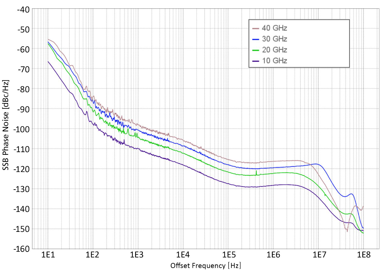
5Phase Noise & Spectral Purity
Phase Noise
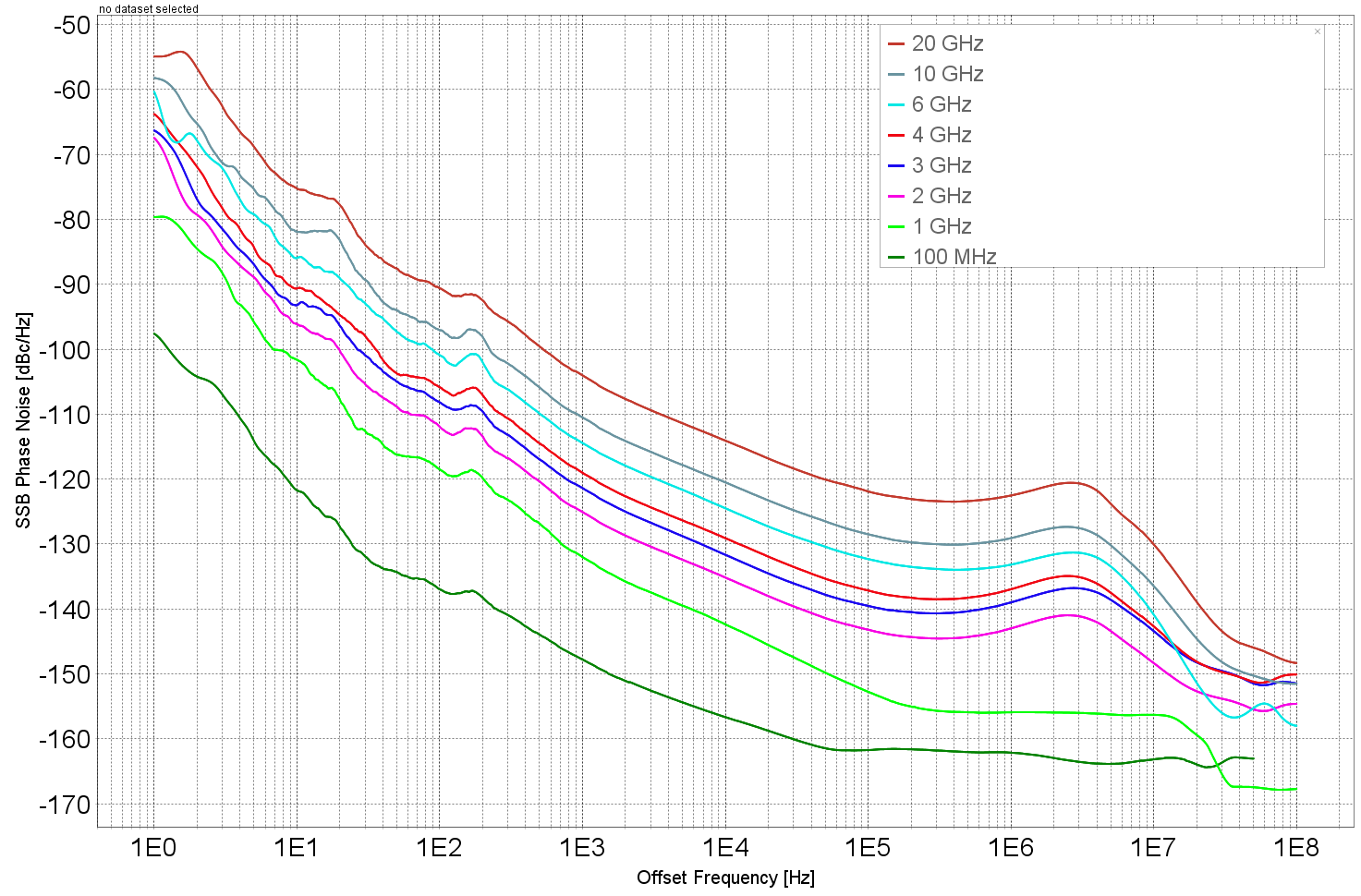
| SSB Phase noise at 1 GHz | Typical | Note |
|---|---|---|
| at 10 Hz from carrier | −93 dBc/Hz | Option LN / LN+ |
| at 1 kHz from carrier | −130 dBc/Hz | |
| at 100 kHz from carrier | −145 dBc/Hz | |
| Wideband noise | −160 dBc/Hz |
| SSB Phase noise at 10 GHz | Typical | Note |
|---|---|---|
| at 10 Hz from carrier | −73 dBc/Hz | Option LN / LN+ |
| at 1 kHz from carrier | −110 dBc/Hz | |
| at 100 kHz from carrier | −125 dBc/Hz | |
| Wideband noise | −160 dBc/Hz |
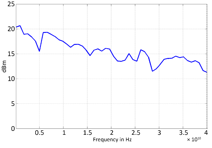
Spectral Purity
| Output harmonics @ 5 dBm | Typical | Max | Note |
|---|---|---|---|
| < 1.2 GHz | −25 dBc | −20 dBc | (see also plots) |
| 1.2 to 2.5 GHz | −15 dBc | −9 dBc | |
| 2.5 to 5 GHz | −30 dBc | −23 dBc | |
| 5 to 12 GHz | −15 dBc | −9 dBc | |
| 12 to 20 GHz | −25 dBc | −20 dBc | |
| > 20 GHz | −20 dBc | −12 dBc |
| Output harmonics @ 0 dBm (Option FILT) | Typical | Max |
|---|---|---|
| < 1 GHz | −35 dBc | −25 dBc |
| > 1 GHz | −55 dBc | −45 dBc |
| Sub-harmonics @ 5 dBm | Typical | Max |
|---|---|---|
| < 20 GHz | −75 dBc | −55 dBc |
| > 20 GHz | −50 dBc | −25 dBc |
| Non-harmonic spurious @ 5 dBm (CW, offset from 10 kHz until 500 MHz) | Typical | Max |
|---|---|---|
| < 1.2 GHz | −90 dBc | −55 dBc |
| 1.2 – 2.5 GHz | −85 dBc | −55 dBc |
| 2.5 – 5 GHz | −80 dBc | −55 dBc |
| 5 – 10 GHz | −75 dBc | −55 dBc |
| 10 – 20 GHz | −70 dBc | −50 dBc |
| > 20 GHz | −65 dBc |
6Modulation
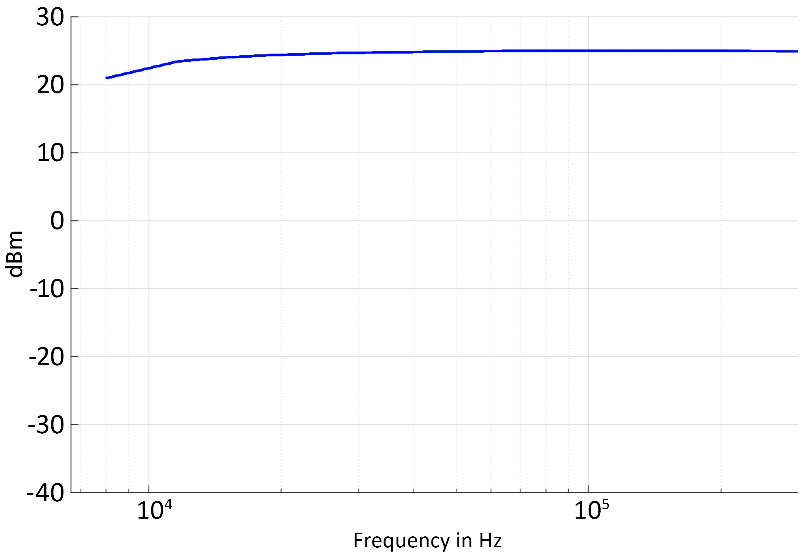
Pulse Modulation
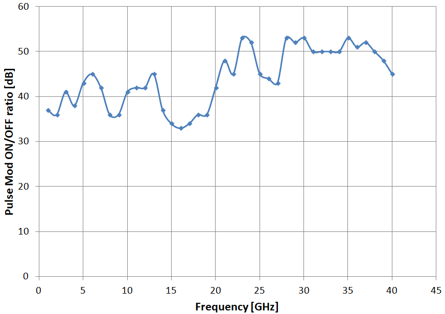
| Parameter | Min | Typical | Max | Note |
|---|---|---|---|---|
| Modulation source | Internal / External | |||
| Pulse rise/fall time | 10 ns | |||
| On/off ratio | 25 dB | 40 dB | Pout > +10 dBm, see plot | |
| Pulse overshoot | 10% | |||
| Pulse delay | 20 ns | |||
| Pulse polarity | Normal, inverse selectable | |||
| External input threshold | 0.85 V | 0.9 V | 0.95 V | TTL compatible |
| External input voltage range | −0.5 V | +5.5 V | TTL compatible | |
| External input hysteresis | 60 mV |
Internal Pulse Generator
| Parameter | Min | Typical | Max | Note |
|---|---|---|---|---|
| Repetition frequency (PRF) | 0.1 Hz | 100 MHz | = 1/T | |
| Duty cycle | 1 % | 99 % | in 1% steps, within specified minimum pulse width | |
| Minimum pulse settling range | 30 ns | 20 s | ||
| Pulse Pattern Modulation & Staggered PRF | Using internal pattern generator | |||
| Pulse width | 30 ns | 5 s | ||
| Programmable pattern length | 2 | 65536 | ||
| Duty cycle | 0.05% | 99.95% | ||
| Pulse width resolution | 5 ns | |||
| Pulse period (T) accuracy | 0.00005×T + 3 ns | |||
| Pulse width accuracy | 0.00005×T + 5 ns | |||
| Pulse jitter | < 100 ps | 1 ns | ||
| Polarity | selectable |
Frequency Modulation
| Parameter | Min | Typical | Max | Note |
|---|---|---|---|---|
| Modulation source | Internal | |||
| Maximum Frequency deviation (peak) | N · 400 MHz | < 1.25 GHz (N=1); 1.25 to 2.5 GHz (N=0.125); 2.5 to 5 GHz (N=0.25); 5 to 10 GHz (N=0.5); 10 to 20 GHz (N=1); 20 to 40 GHz (N=2) | ||
| Deviation accuracy | 0.50% | 2% | ||
| Distortion (THD) | < 1 % | 1 kHz rate, 10 kHz deviation | ||
| Modulation rate | 0.1 Hz | 80 kHz | ||
| Modulation waveforms | Sine |
Phase Modulation
| Parameter | Min | Typical | Max | Note |
|---|---|---|---|---|
| Modulation source | Internal | |||
| Phase deviation (peak) | 0 | 300 · N · rad | ||
| Deviation accuracy | 0.50% | 2% | ||
| Modulation rate | 0.1 Hz | 80 kHz | ||
| Modulation waveforms | Sine | |||
| Distortion (THD) | < 1% | 1 kHz rate & N x rad deviation |
7Sweep & Trigger
Sweeping Capability
Sweep type: linear, logarithmic, random.
| Frequency Sweep | Typical | Note |
|---|---|---|
| Step time (tstep) | 500 µs 20 µs | Option FS |
| Dwell time (tdwell) | 15 µs |
Trigger (TRIG IN): Input is TRIG IN at front panel
| Parameter | Min | Typical | Max | Note |
|---|---|---|---|---|
| Trigger Types | Continuous, single (point), gated, gated direction | |||
| Trigger Source | external, bus (LAN, USB) | |||
| Trigger Modes | Continuous free run, trigger and run, reset and run | |||
| Trigger latency | 5 ns | |||
| Trigger uncertainty | 10 ns | |||
| External Trigger delay | 50 ns | 40 s | ||
| External Delay Resolution | 5 ns | |||
| Trigger Modulo | 1 | 255 | Execute only on Nth trigger event | |
| Trigger Polarity | Rising, falling | |||
| External trigger input threshold | 0.85 V | 0.9 V | 0.95 V | TTL compatible |
| External trigger input voltage range | −0.5 V | +5.5 V | TTL compatible | |
| External trigger input hysteresis | 60 mV |
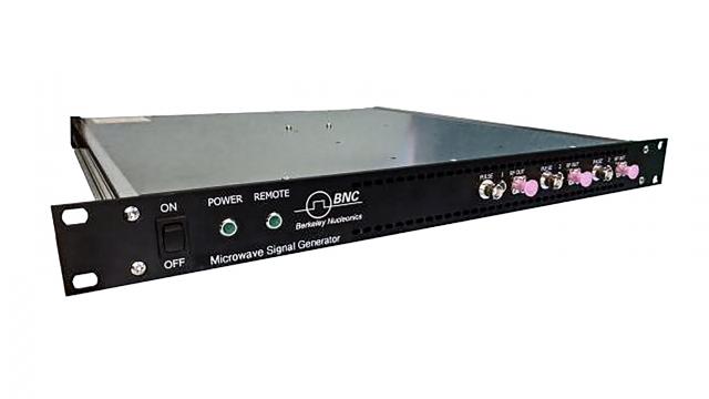
8Connectors & Casings
Front Connectors

- DC power switch
- External pulse modulation inputs: BNC female (1 to 4)
- RF outputs: K (2.92 mm) female (1 to 4)
Rear Connectors

- Unit-to-unit synchronization signal input (SYNC IN): SMA female
- Unit-to-unit synchronization signal output (SYNC OUT): SMA female
- High Stability Reference input (CLK IN, 3 GHz): SMA female
- High Stability Reference output (CLK OUT, 3 GHz): SMA female
- Trigger output (TRIG OUT): BNC female
- Trigger input (TRIG IN): BNC female
- Reference output (REF OUT): BNC female
- Reference input (REF IN): BNC female
- GPIB: IEEE-488.2, 1987 with listen and talk (optional)
- LAN connection: RJ-45
- USB 2.0 device
- FUSE (3.15 A)
- 100-240V AC power plug
Casings

Standard 19″ 1U casing. High Isolation Casing 19″ 1U is available as option HI (rack mount kit included).

9General Characteristics
| Parameter | Specification |
|---|---|
| Remote programming interfaces | Ethernet 100BaseT LAN interface, USB 2.0 host & device, GPIB (IEEE-488.2, 1987) with listen and talk (optional), Control language SCPI Version 1999.0 |
| Power requirements | 24V ± 3.0 VDC; 25 W maximum |
| Mains adapter supplied | 100-240 VAC in / 24 V 4.0 A DC out |
| Environmental | Levels similar to MIL-PRF-28800F Class 3/4 |
| Operating temperature range | 0 to 45 °C |
| Storage temperature range | −40 to 70 °C |
| Operating and storage altitude | up to 15,000 feet (4600 m) |
| Safety / EMC | Complies with applicable Safety and EMC regulations and directives |
| Weight | ≤ 10.0 kg (22 lbs) net |
| Dimensions (19″ 1U enclosure) | 43 mm H x 426 mm W x 460 mm L [1.7 in H x 16.8 in W x 18.1 in L] |
10Ordering Information
| Product | Description |
|---|---|
| 865B-M-1 | Single output, 19″ 1U rack-mount module |
| 865B-M-2 | Dual-Output, 19″ 1U rack-mount module |
| 865B-M-3 | Triple-Output, 19″ 1U rack-mount module |
| 865B-M-4 | Quad-Output, 19″ 1U rack-mount module |
| Option LN | Enhanced close in phase noise & frequency stability |
| Option LN+ | Enhanced close in phase noise & further enhanced long term frequency stability |
| Option FS | Ultra-fast switching speed |
| Option VREF | Variable external reference |
| Option GPIB | GPIB interface |
| Option HI | High isolation 19″ 1U casing |
| Option FILT | Enhanced harmonic rejection |
| Option 8K | Frequency range extension to 8 kHz |
For configuration help, pricing, or a quotation, contact Berkeley Nucleonics at info@berkeleynucleonics.com or 415-453-9955.
11Applications
- ATE (Automated Test Equipment)
- LO for Frequency Converters
- Telecom / SatCom
- System Integration