Model 855B Multi-Channel RF and Microwave Signal Generators
A 1U rackmount, ultra-low phase noise, phase-coherent multi-channel signal generator with ultra-fast switching, high output power, and very stable phase coherence across all channels.
Model 855B · 300 kHz to 6, 12, 20, 33 and 40 GHz · up to 4 channels · Data Sheet
1Overview
The Model 855B is a phase-coherent, multi-channel, high output power, ultra-fast switching and ultra-low phase noise signal generator with a frequency range from 300 kHz to 6, 12, 20, 33 or 40 GHz. It suits a wide range of applications where good signal quality, accurate and wide output power ranges, and very stable phase coherence among all channels are required. Excellent phase noise is combined with good spurious, harmonic rejection and optionally leading-edge switching speed of 25 µs.
A high-stability OCXO reference provides excellent frequency accuracy and stability. The generator accepts a wide range of external references including the commonly used 10 and 100 MHz, and a flexible reference choice in the range of 1 to 250 MHz for customer- or system-specific reference frequencies. The Model 855B also features a pair of BNC-specific high-frequency CLK ports (one input and one output) that enable excellent phase synchronization among the outputs from multiple 855B modules.
The Model 855B comes in a standard 19 inch 1U (up to 4 channels) rack-mountable module form. It can be controlled by a PC-based GUI software and offers USB, LAN or GPIB interfaces, each using the SCPI 1999 command set. A customer-supplied API or programming examples for Matlab, Labview, C++ and other tools make control implementation straightforward.
2Key Features
Very low phase noise.
Industry lowest phase drift.
Ultra-fast switching.
Phase-coherent switching option.
Multi-channel phase-coherent outputs.
Variable external clock reference output.
Applications
Radar simulation.
Quantum computing.
High volume automated testing.
Phased array antenna / beamforming.
Electronic warfare.
SatCom R&D.
3Frequency & Output Power
Frequency Parameters / Range
Parameter
Min
Max
Note
Frequency Range
855B-06
300 kHz
6 GHz
855B-12
300 kHz
12 GHz
855B-20
300 kHz
20 GHz
855B-33
300 kHz
33 GHz
855B-40
300 kHz
40 GHz
Resolution
<0.001 Hz (typical)
Phase Adjustment Range
0 deg
360 deg
Individually adjustable per channel
Phase Resolution
0.1 deg (typical)
Level Performance
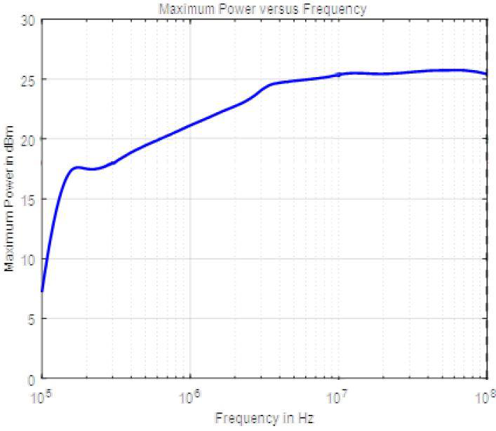
Figure 6: Low frequency response 855B-20 (100 kHz to 100 MHz).
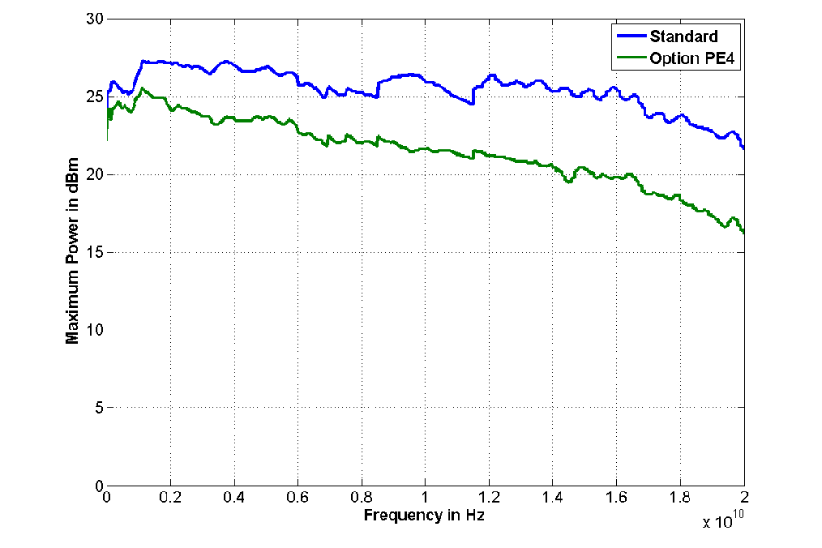
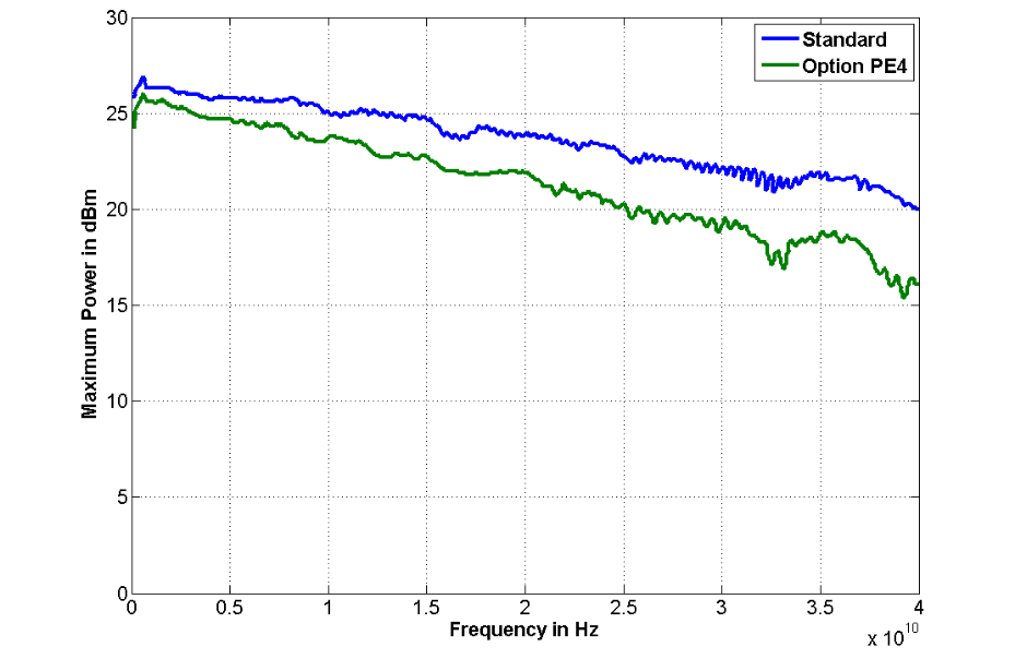
Output power level varies by frequency band. With option PE4 an electrical step attenuator extends the floor to -80 dBm (855B-06/12/20) or -50 dBm (855B-33/40).
Output Power Level
Min
Max
Note
Output Power Level 855B/06/12/20/33/40G
< 100 MHz
-20 dBm
+20 dBm
100 MHz to 6 GHz
-20 dBm
+25 dBm
6 GHz to 18 GHz
-20 dBm
+23 dBm
18 GHz to 20 GHz
-20 dBm
+20 dBm
20 GHz to 40 GHz
-20 dBm
+18 dBm
Output Power Level 855B-06/12/20G
Option PE4
10 MHz to 12 GHz
-80 dBm
+20 dBm
12 GHz to 15 GHz
-80 dBm
+18 dBm
15 GHz to 20 GHz
-80 dBm
+15 dBm
Output Power Level 855B-33/40
Option PE4
10 MHz to 20 GHz
-50 dBm
+19 dBm
20 to 33 GHz
-50 dBm
+16 dBm
33 to 40 GHz
-50 dBm
+15 dBm
Power Resolution
0.01 dB (typical)
Thermal Drift
0.015 dB/°C (typical)
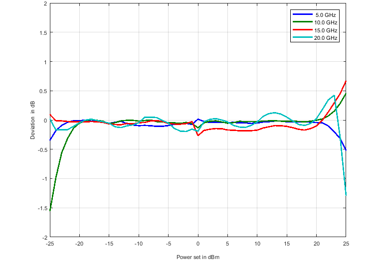
Figure 4: Maximum output power 855B-20 with and without option PE4.Figure 5: Maximum output power 855B-40 with and without option PE4.
Relative Power Error (0.1 dB Step)
Values in parentheses are typical.
Frequency
Min Power to -50 dBm (PE4)
-50 to -20 dBm (PE4)
-20 to +15 dBm
+15 dBm to Max Power
300 kHz to 20 GHz
(< 0.1 dB)
0.5 dB (< 0.1 dB)
0.5 dB (< 0.1 dB)
(< 0.1 dB)
20 to 26 GHz
N/A
(< 0.1 dB)
(< 0.1 dB)
(< 0.1 dB)
26 to 40 GHz
N/A
(<0.1 dB)3
(< 0.1 dB)
(< 0.1 dB)
Power Level Uncertainty
Values in parentheses are typical.
Frequency
Min Power to -50 dBm (PE4)
-50 to -15 dBm (PE4)
-15 to +15 dBm
+15 dBm to Max Power
< 6 GHz
(4 dB)
1.2 dB
0.8 dB (0.25 dB)
1.2 dB
6 to 12 GHz
(4 dB)
1.3 dB
0.9 dB (0.3 dB)
1.3 dB
12 to 26 GHz
(4 dB)
2.0 dB
1.0 dB (0.3 dB)
2.0 dB
26 to 40 GHz
N/A
2.3 dB
1.2 dB (0.4 dB)
2.3 dB
2 Applies to devices with Serial Number >= ###-#########-0888 and to devices with Option PL. 3 Applies to the range -45 dBm to -20 dBm.
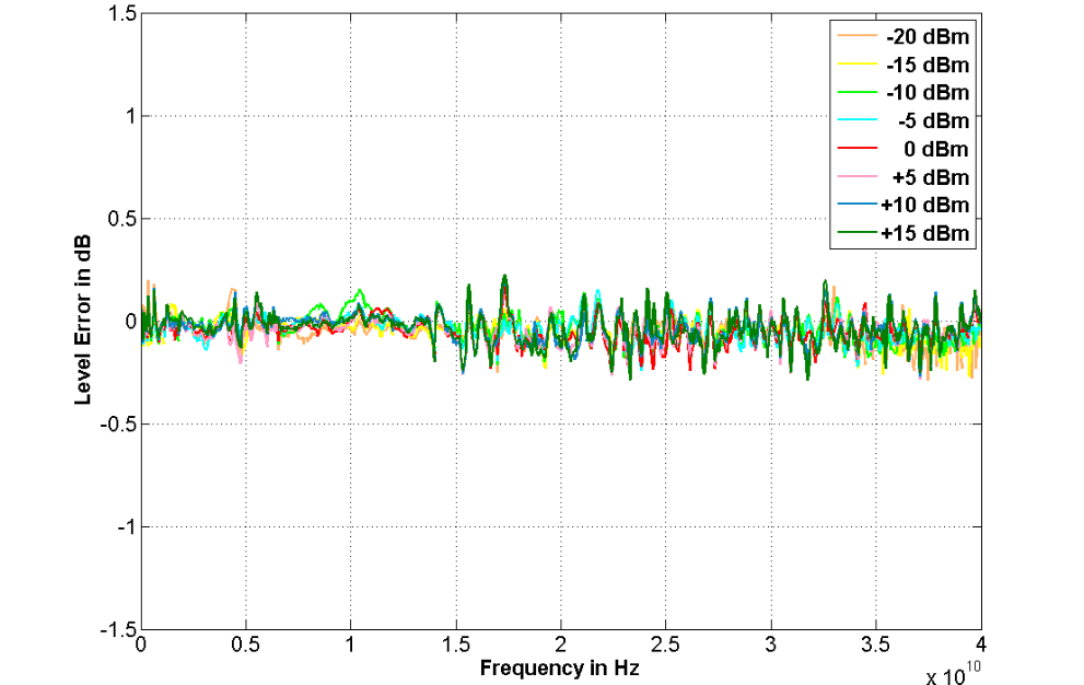
Figure 7: Level error (300 kHz to 40 GHz, 855B-40).Figure 8: Level linearity.Figure 9: Level linearity with option PE4.
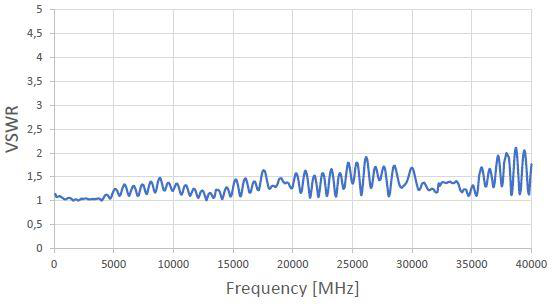
Reverse Power Protection and VSWR
Parameter
Typical
Max
Note
Reverse Power Protection
DC Voltage
±10 V
RF Power
26 dBm
Output Impedance
50 Ohms
VSWR
< 15 GHz
1.3
1.5
15 to 35 GHz
1.6
1.8
> 35 GHz
1.9
2.2
Figure 10: VSWR.
4Phase Noise & Spectral Purity
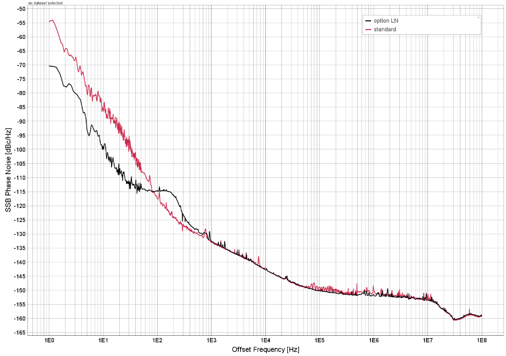
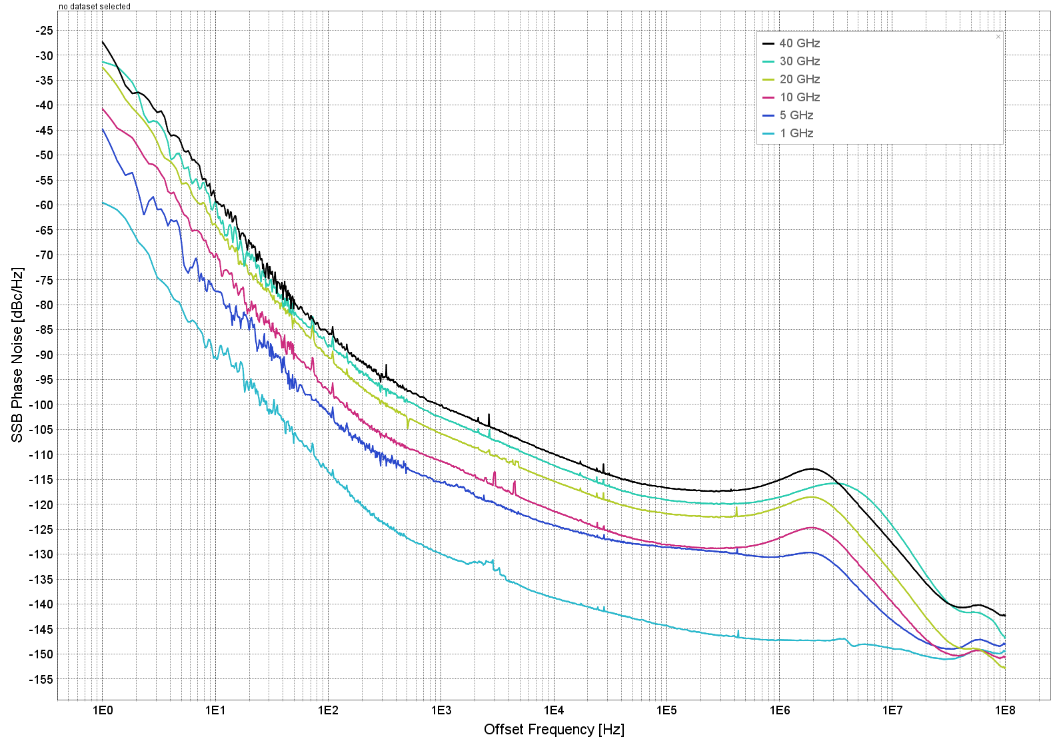
Phase Noise
SSB phase noise at maximum output power, ALC off. Option LN improves close-in performance at each carrier frequency.
Parameter (SSB Phase Noise)
Typical
Max
Note
SSB Phase noise at 1 GHz
See plots/tables. Max output power, ALC Off
At 10 Hz from carrier
-87 dBc/Hz
-76 dBc/Hz
At 10 Hz from carrier
-98 dBc/Hz
-86 dBc/Hz
Option LN
At 1 kHz from carrier
-130 dBc/Hz
-125 dBc/Hz
At 100 kHz from carrier
-145 dBc/Hz
-140 dBc/Hz
SSB Phase Noise at 4 GHz
Max output power, ALC Off
At 10 Hz from carrier
-74 dBc/Hz
-68 dBc/Hz
At 10 Hz from carrier
-85 dBc/Hz
-74 dBc/Hz
Option LN
At 1 kHz from carrier
-116 dBc/Hz
-111 dBc/Hz1
At 100 kHz from carrier
-136 dBc/Hz
-131 dBc/Hz
SSB Phase noise at 10 GHz
Max output power, ALC Off
At 10 Hz from carrier
-67 dBc/Hz
-60 dBc/Hz
At 10 Hz from carrier
-77 dBc/Hz
-66 dBc/Hz
Option LN
At 1 kHz from carrier
-108 dBc/Hz
-103 dBc/Hz
At 100 kHz from carrier
-127 dBc/Hz
-122 dBc/Hz
1 With option PHS, the phase noise for offsets >= 100 Hz at frequencies between 1.1 GHz and 10 GHz is typically 10 dB higher.
Figure 1: Phase noise with and without option LN (at 1 GHz and max. output power).Figure 2: Phase noise without option LN (at max. output power).
Spectral Purity
Parameter
Typical
Max
Note
Harmonics 6, 12, 20G
At +5 dBm output power
50 to 200 MHz
-30 dBc
-20 dBc
200 to 600 MHz
-35 dBc
-25 dBc
600 MHz to 6 GHz
-40 dBc
-30 dBc
6 to 30 GHz
-35 dBc
-25 dBc
Harmonics 33, 40G
50 to 200 MHz
-30 dBc
-20 dBc
200 MHz to 12 GHz
-35 dBc
-30 dBc
12 to 20 GHz
-30 dBc
-20 dBc
> 20 GHz
-25 dBc
Sub-Harmonics
< 5 GHz
-75 dBc
-70 dBc
5 to 20 GHz
-70 dBc
-65 dBc
> 20 GHz
-55 dBc
Non-Harmonic Spurious
> 10 kHz offset
< 1.2 GHz
-90 dBc
-60 dBc
1.2 to 2.5 GHz
-92 dBc
-60 dBc
2.5 to 5 GHz
-87 dBc
-60 dBc
5 to 10 GHz
-80 dBc
-60 dBc
10 to 20 GHz
-75 dBc
-50 dBc
20 to 40 GHz
-67 dBc
Figure 3: 855B / 40G harmonic performance.
5Modulation
The 855B provides pulse modulation, including an internal pulse generator and pulse pattern modulation with staggered PRF. Option MOD adds amplitude, frequency, and phase modulation.
< 1.25 GHz (N=1); 1.25 to 2.5 GHz (N=0.125); 2.5 to 5 GHz (N=0.25); 5 to 10 GHz (N=0.5); 10 to 20 GHz (N=1); 20 to 40 GHz (N=2)
Deviation Accuracy
0.50%
2%
Distortion (THD)
< 1%
1 kHz rate, 10 kHz deviation
Modulation rate
0.1 Hz
80 kHz
Modulation waveforms
Sine
Phase Modulation (Option MOD)
Parameter
Min
Typical
Max
Note
Modulation Source
Internal
Phase deviation (peak)
0
300 · N · rad
Deviation Accuracy
0.50%
2%
Modulation rate
0.1 Hz
80 kHz
Modulation waveforms
Sine
Distortion (THD)
< 1%
1 kHz rate & N x rad deviation
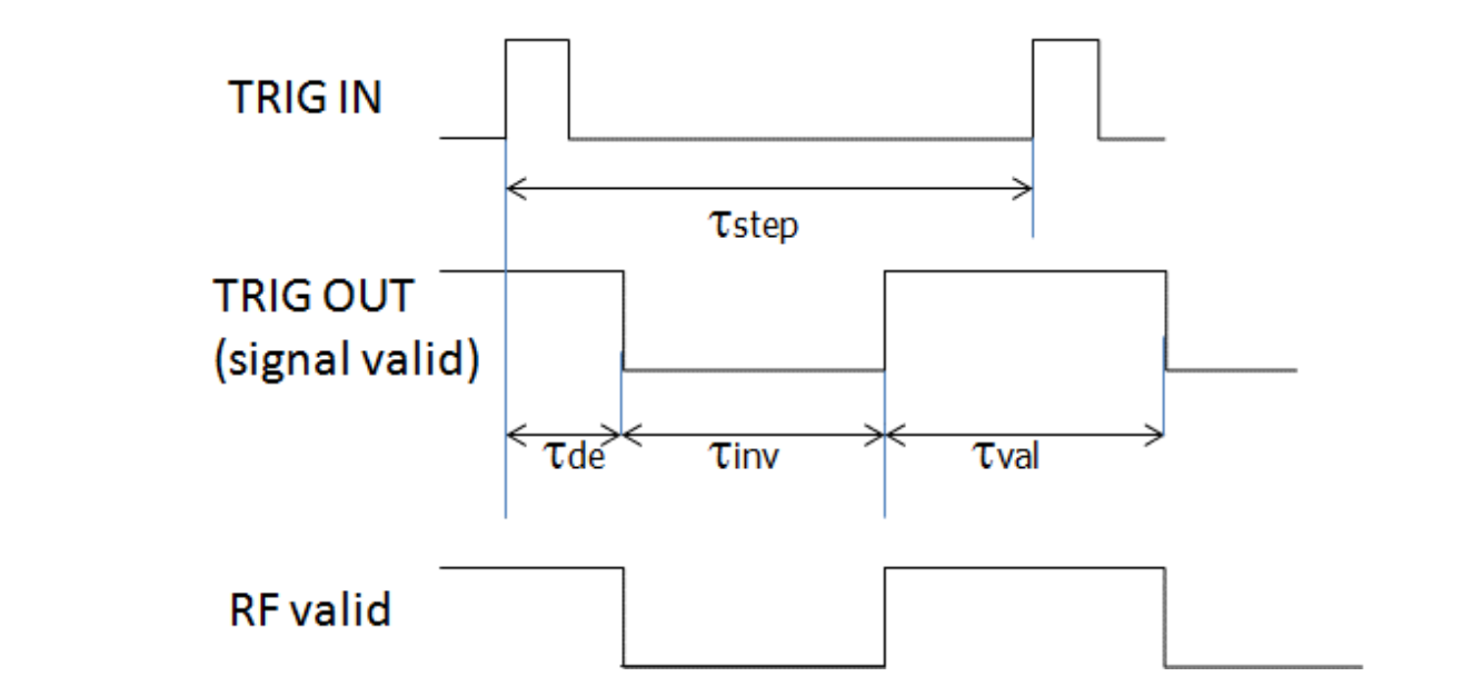
6Switching, Sweep & Reference
Switching Speed
Parameter
Typical
Note
Switching Speed
After SCPI command received
CW Mode
1.5 ms
Sweep/List mode
500 µs
25 µs
Option FS
Sweeping Capability
Parameter
Min
Typical
Max
Note
Sweep Parameters
Frequency, power, phase, list
Sweep type
Linear, logarithmic, random
Step time (tstep)
500 µs
19998 s
Standard
f < 31.8 GHz, fstep < 2.2 GHz
25 µs
Option FS (1, 2 channels)4 in band
50 µs
Option FS (3, 4 channels)4 in band
<=70 µs
Option FS cross band
f < 31.8 GHz, fstep >= 2.2 GHz
30 µs
Option NEC (1, 2 channels)4 in band
50 µs
Option NEC (3, 4 channels)4 in band
<=70 µs
Option NEC cross band
f >= 31.8 GHz, fstep < 0.55 GHz
100 µs
Option NEC (1 to 4 channels)4
30 µs
Option NEC (1, 2 channels)4 in band
50 µs
Option NEC (3, 4 channels)4 in band
<= 70 µs
Option NEC cross band
f >= 31.8 GHz, fstep >= 0.55 GHz
500 µs
Option NEC (1 to 4 channels)
Dwell time (tdwell)
15 µs
9999 s
Off time (toff)
15 µs
9999 s
Time resolution
5 ns
Timing delay (Tde)
50 ns
Transient time (Tinv)
25 µs
Timing accuracy per point
5 ns
Number of points
2
10000
Per channel
Sweep timing: TRIG IN, TRIG OUT (signal valid) and RF valid, showing τstep, τde, τinv and τval.
Frequency Reference
Parameter
Typical
Note
Internal Reference Frequency
100 MHz
Internal Reference Frequency
10 MHz
Option LN
Temperature stability 0 to 50 degC
±100 ppb
Temperature stability 0 to 50 degC
±20 ppb
Option LN
Aging 1st year
1000 ppb
Aging 1st year
30 ppb
Option LN
Aging 1st year
20 ppb
Option LN+
Aging per day
5 ppb
After 30 days operations
Aging per day
0.5 ppb
Option LN
Warm-up time
5 min
Output of internal reference
10 MHz / 100 MHz
REF OUT port, selectable
Output of High Frequency Clock
3 GHz
CLK OUT port
Output power (high phase synchronous mode)
0 dBm
10 MHz, 3 GHz
Output power
9 dBm
100 MHz
Output impedance
50 Ohms
Bypass Internal Reference Input
100, 1000 MHz
*Options LN/LN+ are bypassed
Phase Lock to External Reference
10 MHz integer MHz (1 MHz to 250 MHz)
REF IN port, Option VREF. *Options LN/LN+ are bypassed
High Frequency Clock Input (Bypass Internal Reference)
3 GHz
CLK IN port, high phase synchronous mode
Reference input level: 10 MHz or 1-250 MHz or 3 GHz
0 dBm (-5 to +10 dBm)
Reference input level: 100, 1000 MHz
+5 to +13 dBm
Lock Range: 10 MHz or 1-250 MHz
±1.5 ppm
Lock Range: 100 MHz
100 ppm
Reference input impedance
50 Ohms
Trigger (TRIG IN)
Parameter
Min
Typical
Max
Note
Trigger Types
Continuous; Single (point); Gated; Gated Direction
Trigger Source
External; Bus (LAN, USB)
Trigger Modes
Continuous free run; Trigger and run; Reset and Run
Trigger Latency
5 ns
Trigger Uncertainty
10 ns
External Trigger delay
50 ns
40 s
settable
External delay resolution
5 ns
Trigger modulo
1
255
Execute only on Nth trigger event
Trigger Polarity
Rising; Falling
External trigger input threshold
0.85 V
0.9 V
0.95 V
TTL Compatible
External trigger input voltage range
-0.5 V
+5.5 V
TTL Compatible
External trigger input hysteresis
60 mV
Multi-Purpose Output (FUNC OUT)
Output is TRIG OUT at the rear panel. Multifunction generator: sine, triangle, square wave.
Parameter
Min
Typical
Max
Note
Frequency range
1 Hz
3 MHz
Sine
Frequency range
1 Hz
1 MHz
Triangle
Frequency range
50 kHz
Square
Frequency resolution
0.1 Hz
Output voltage amplitude peak-peak
10 mV
2 V
Sine, triangle
Output voltage amplitude peak-peak
5 V
Square (CMOS output)
Harmonic Distortion
1%
< 100 kHz, 1 Vpp
Output impedance
50 Ohms / CMOS
Sine, triangle / Square wave
Video output (of internal pulse modulator)
CMOS; Period 30 ns to 50 s; Pulse width 15 ns to 50 s; RF delay 10 ns
Trigger out modes
Trigger on sweep start; Trigger on each point; Signal Valid
Synchronization mode for multiple sources
4 In band / cross band as noted per option and channel count.
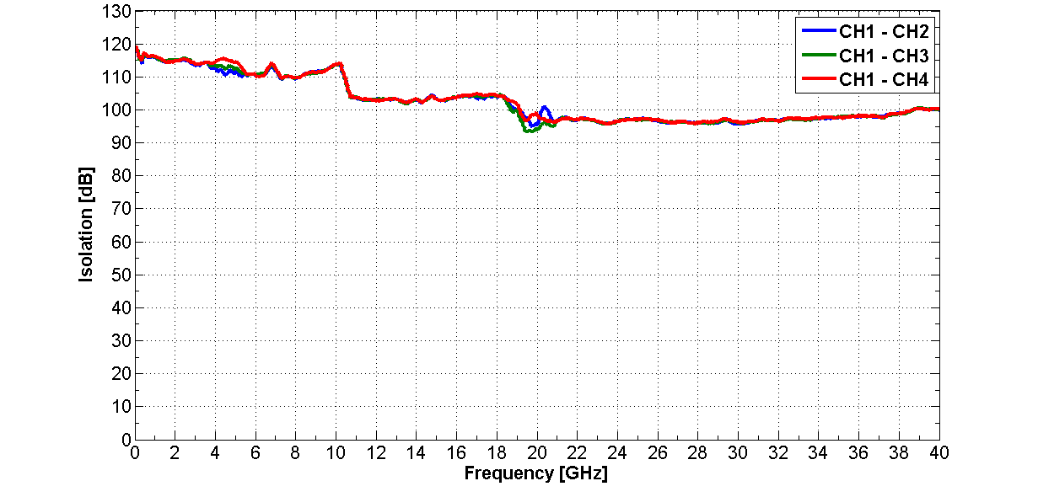
6bChannel-to-Channel Performance
Parameter
Min
Typical
Note
Isolation
< 3 GHz
90 dB
3 to 6.5 GHz
70 dB
80 dB
> 6 GHz
> 60 dB
300 kHz to 40 GHz
80 dB
> 90 dB
Option HI, see plot
Relative Phase Stability between Channels
0.096 ps
3 mrad at 5 GHz over 5 hours
Relative Phase Stability between Synchronized Modules
0.160 ps
5 mrad at 5 GHz over 5 hours
Phase-Coherent Switching
Phase mismatch at outputs
15 ps
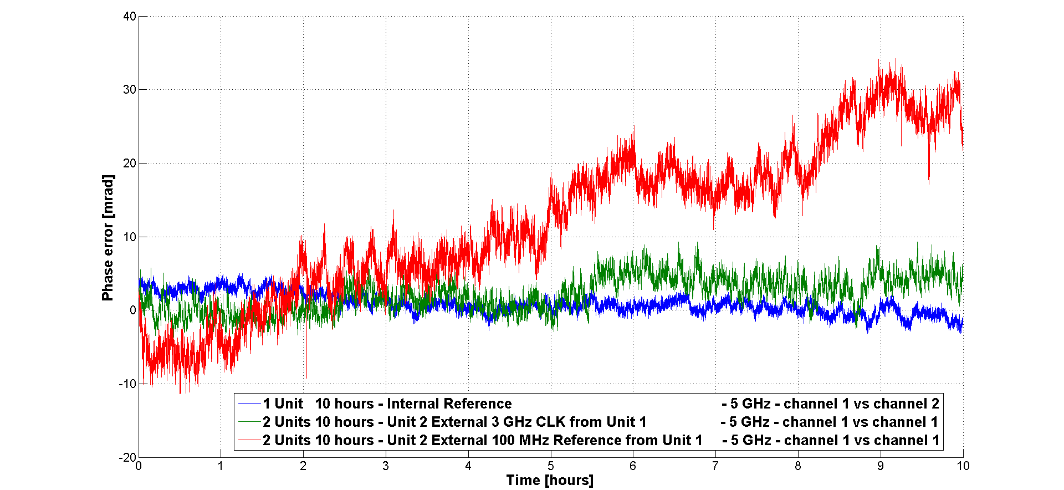
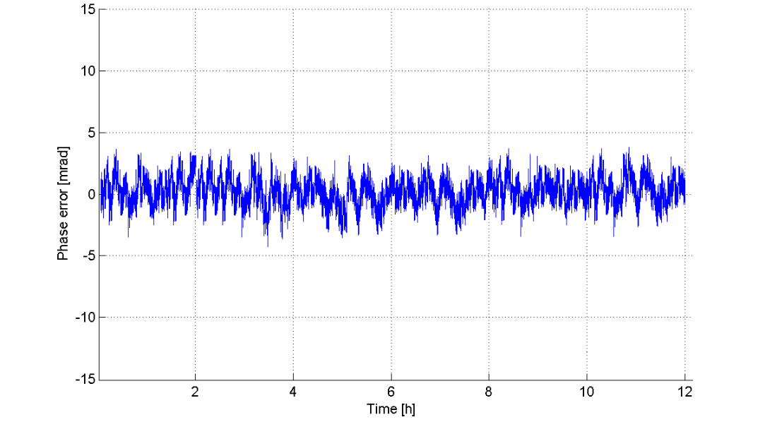
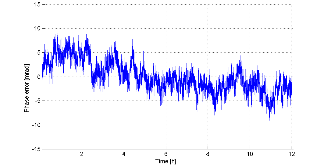
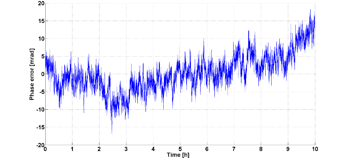
Figure 11: Channel-to-channel isolation with option HI (channel under test: channel 1 at frequency f, power 10 dBm; channels 2, 3 and 4 at f + 9 MHz, power 10 dBm; measurement made on channel 1 at f + 9 MHz).Figure 12: Channel-to-channel phase stability under different test conditions.Figure 13: 855B-20 typical time domain channel-to-channel phase error at 10 GHz.Figure 14: 855B-20 typical time domain channel-to-channel phase error at 20 GHz.Figure 15: 855B-40 typical time domain channel-to-channel phase error at 38 GHz.
7General Characteristics
Parameter
Specification
Remote programming interfaces
Ethernet 100BaseT LAN; USB 2.0 device; GPIB (IEEE-488.2, 1987) with listen and talk (Option GPIB)
Control language
SCPI Version 1999.0
Power requirements
100 - 240 VAC, 50 or 60 Hz, 160W maximum (80W + 20W per channel)
Environmental
Levels similar to MIL-PRF-28800F Class ¾
Safety / EMC
Complies with applicable Safety and EMC regulations and directives
Weight
21 lbs [≤ 10.0 kg] net
Dimensions, 19” 1U enclosure (855B-06/12/20)
1.7 in H x 16.8 in W x 18.3 in L [44 mm H x 426 mm W x 465 mm]
Dimensions, 19” 1U enclosure (855B-33/40)
1.7 in H x 16.8 in W x 19.1 in L [44 mm H x 426 mm W x 485 mm]
Dimensions, 19” 1U HI enclosure
1.7 in H x 17.3 in W x 18.5 in L [44 mm H x 440 mm W x 470 mm L]
Definitions. Specifications describe the warranted performance of the instrument for 23 ±5 °C after a 30-minute warm-up period (unless otherwise stated). Min/Max: parameter range guaranteed by product design and/or production tested, including guard-bands. Typical: expected mean values, not warranted performance.
8Connectors & Form Factor
The 855B is controlled through USB, LAN or GPIB, all using the SCPI 1999 command set. Dedicated 3 GHz CLK I/O ports synchronize multiple units, so phase-coherent test setups can scale across multiple modules. Up to 4 channels fit a standard 19 inch 1U enclosure. A high-isolation chassis is available with option HI.
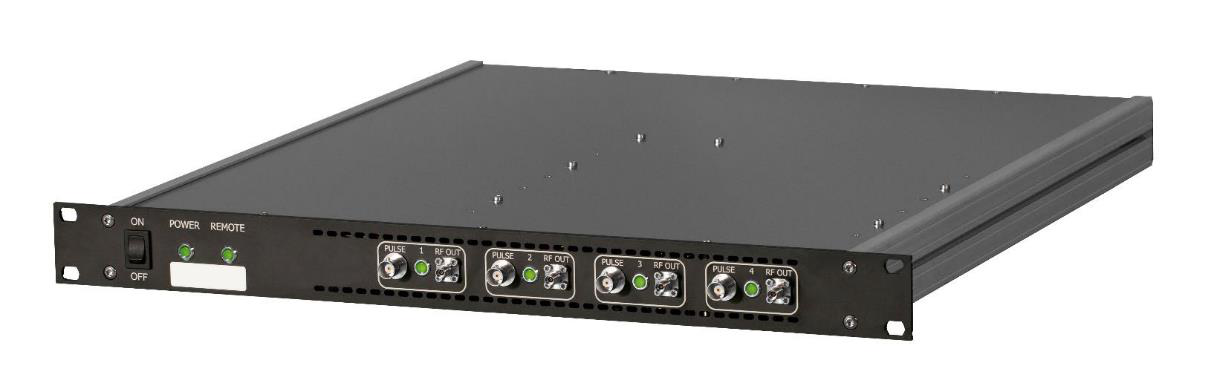
Connectors (Front)
Model 855-R four-channel front panel: power switch, status LEDs, and RF OUT 1 to 4.
Power Switch.
LED Indicator: Power ON; Remote; RF ON (per channel).
RF Outputs: 855B-33, 40: K (2.92 mm) female; 855B-06, 12, 20: SMA female.
External pulse modulation inputs: BNC female.
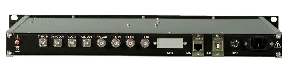
Connectors (Rear)
Rear panel: SYNC IN/OUT, CLK IN/OUT, TRIG OUT/IN, REF OUT/IN, GPIB, LAN, USB, fuse and AC power.
Unit-to-unit synchronization signal input (SYNC IN): SMA female.5
Unit-to-unit synchronization signal output (SYNC OUT): SMA female.5
High Stability Reference input (CLK IN, 3 GHz): SMA female.
High Stability Reference output (CLK OUT, 3 GHz): SMA female.
Trigger output (TRIG OUT): BNC female.
Trigger input (TRIG IN): BNC female.
Reference input (REF IN): BNC female.
GPIB: IEEE-488.2, 1987 with listen and talk (optional).
LAN connection: RJ-45.
USB 2.0 device.
FUSE (3.15 A).
100-240V AC power plug.
5 Allows to extend option PHS over multiple units (unreleased).
Casings Standard 19” 1U
Standard 19” 1U casing (up to 4 channels), front panel with power switch, POWER and REMOTE indicators, and per-channel PULSE and RF OUT connectors.
High Isolation Casing 19” 1U (Option HI, rack mount kit included)
High Isolation 19” 1U casing (Option HI), rack mount kit included.
9Options & Configurations
Option
Description
LN
Enhanced close in phase noise and frequency stability
LN+
Option LN with improved long term frequency stability
PE4-12
Electrical step attenuator (6 & 12 GHz version)
PE4-20
Electrical step attenuator (20 GHz version)
PE4-40
Electrical step attenuator (33 & 40 GHz version)
PHS
Phase coherent switching
FS
Ultra-fast switching speed
MOD
Amplitude, frequency, phase modulations added
VREF
Flexible external reference frequency support in range 1 to 250 MHz
GPIB
GPIB interface
FLASH
MicroSD card slot for removable SD memory
HI
High isolation 19” 1U casing (highly improved channel-to-channel isolation)
IEC
IEC 17025 Calibration with Certificate
Retrofit
Applies when options are back-ordered
10Applications
Radar simulation and phased-array antenna or beamforming test.
Quantum computing.
High-volume automated testing.
Electronic warfare.
Satellite communications R&D.
11Ordering
Specify the frequency variant (855B-6 through 855B-40), channel count, chassis size, and options when requesting a quote. For configuration help, pricing, or a demonstration, contact Berkeley Nucleonics.
Configuration note. Channel count, chassis size, phase-noise grade, and per-output frequency ranges are configurable. Confirm the exact build and all performance figures against the released Model 855B datasheet (v1.74) before ordering.