1Overview
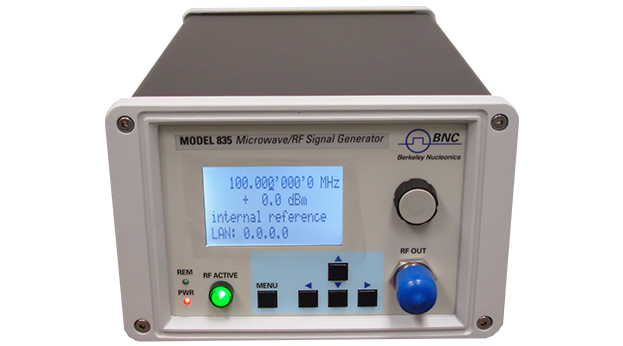
The Model 835 models comprise a set of very compact, portable analog signal generator models from 9 kHz up to 6100 MHz. A combination of good signal purity, fast switching speed and wide dynamic range makes these units useful for a variety of applications.
The Model 835 is a series of low-noise and fast-switching analogue signal generators covering a frequency range from 9 kHz up to 4.0, and 6.1 GHz, respectively. It provides full RF signal generator capabilities including OCXO-stabilized low phase-noise signal with micro-Hz frequency resolution, wide and accurately levelled output power range, extensive modulation capabilities, and fast switching. It is targeted for a wide range of applications where a high-quality analogue signal is mandatory, offering an alternative to expensive high-end RF signal generators, where small size and excellent RF performance at an attractive cost is required.
The very compact and rugged design operates at very low DC power consumption (only 12 watts), with minor heat dissipation and not requiring a noisy fan. This gives the Model 835 a great advantage in laboratories or production test facilities. The low power design allows the use of optional internal battery modules which make it a truly portable instrument, ideally suited for field testing, installation, and maintenance.
The Model 835 supports various standard interfaces such as USB (USBTMC), LAN (VXI-11), or GPIB and extensive API with programming examples are available.
2Key Features
- High output power, low phase noise.
- Comprehensive AM, low-distortion.
- Wideband DC-FM, and high-speed pulse modulation.
- Powerful trigger and sweeping modes.
- Portable battery operation.
3Frequency Parameters / Range
| Parameter | Min | Typical | Max | Note |
|---|---|---|---|---|
| Frequency Range | 9 kHz | 4 GHz 6 GHz | 835-4 835-6 | |
| Resolution | 0.001 Hz | |||
| Phase Resolution | 0.1 deg | |||
| Settling Time | 20 µs 20 µs | 100 µs 200 µs | <= SN xx-xxx2xxxxx-xxxx >= SN xx-xxx3xxxxx-xxxx | |
| Frequency update rate List/sweep mode | 400 µs | 400 µs | time from receipt of SCPI command firmware | |
| Total Jitter | 68 fs RMS | 10 Hz to 1 MHz BW | ||
| Reference frequency input | 8 MHz | 200 MHz | User programmable | |
| Reference input level | -5 dBm | 0 dBm | +13 dBm | |
| Lock Range | +/- 1.0 ppm | |||
| Reference input impedance | 50 Ω | |||
| Internal reference frequency output | 10 MHz | |||
| Initial accuracy of internal reference | ±40 ppb | calibrated at 23 ± 3 °C at time of calibration | ||
| Temperature stability (0 to 50 degC) | ±100 ppb | |||
| Aging 1st year | 0.5 ppm | |||
| Aging per day (after 30 days operations) | 5 ppb | |||
| Warm-Up time | 5 min | |||
| Output of internal reference | +0 dBm | 50 Ω |
4Phase Noise
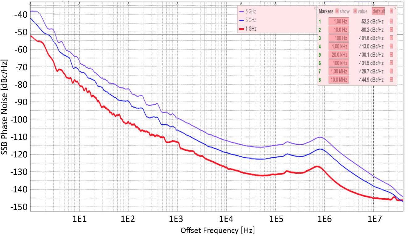
| Parameter | Min | Typical | Max | Note |
|---|---|---|---|---|
| SSB Phase noise | ||||
| At 20 kHz from carrier | -130 dBc/Hz | -128 dBc/Hz | See measured phase noise plots |
5Level Performance
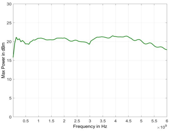
| Parameter | Min | Typical | Max | Note |
|---|---|---|---|---|
| Power Level | See plots on page 8 | |||
| Without Option PE3 | -30 dBm | +18 dBm +17 dBm | >50 MHz & <6 GHz <= 50 MHz | |
| With Option PE3 | -120 dBm | +10 dBm +10 dBm | >50 MHz & <6 GHz <= 50 MHz | |
| Resolution | 0.01 dB | |||
| Level Uncertainty | 0.3 dB 0.5 dB 0.8 dB | < 0.8 dB < 1.3 dB | -20 to + 10 dBm -80 to -20 dBm < -80 dBm |
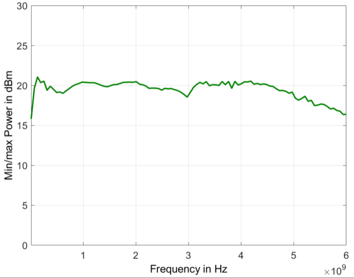
Two leveling paths are available. The standard instrument levels from -30 dBm to +18 dBm above 50 MHz. Option PE3 extends accurate leveling below -120 dBm for receiver sensitivity testing.
6Reverse Power Protection and VSWR
| Parameter | Min | Typical | Max | Note |
|---|---|---|---|---|
| Reverse Power Protection | ||||
| DC Voltage | 30 V | |||
| RF Power | 36 dBm | |||
| Output Impedance | 50 Ω | |||
| VSWR | 1.5 1.7 | 1.8 2.0 | < 3 GHz > 3 GHz |
7Spectral Purity
| Parameter | Min | Typical | Max | Note |
|---|---|---|---|---|
| Spectral Purity | ||||
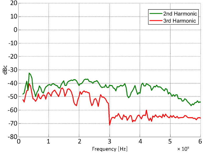
| Output Harmonics > 3.7 GHz Sub-harmonics | -40 dBc -80 dBc | -30 dBc -50 dBc -70 dBc | Pout = +10 dBm Option FILT | |
| Non-harmonic spurious < 1 MHz 1 MHz to 5.8 GHz 5.8 GHz to 6.1 GHz | -70 dBc -65 dBc -60 dBc | -60 dBc -55 dBc -50 dBc | Pout = +10 dBm | |
| Residual FM @ 1 GHz | 3 Hz 12 Hz | 0.3 kHz to 3 kHz, weighted (ITU-T) 0.03 kHz to 23 kHz |
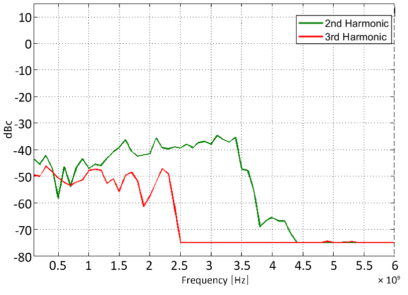
Option FILT adds harmonic filtering that reduces the second and third harmonic across the band, as shown in the filtered harmonic plot.
8Sweeping Capability
Sweeps can be performed with combined internal or external AM/FM/PM/Pulse modulation running. With modulation enabled, the minimum step time increases to 2 ms.
Frequency Sweep
Sweep type: linear, logarithmic, random.
| Parameter | Min | Typical | Max | Note |
|---|---|---|---|---|
| Step time (tstop) | 400 µs | 19998 s | ||
| Dwell time (tdwell) | 50 µs | 9999 s | ||
| Off-time (incl. transient time) (toff) | 0 / 50 µs | 9999 s | ||
| Timing accuracy per point | 1 µs |
Generalized List Sweep
Allows individual setting of frequency, power, dwell-time, and off-time for each point.
| Parameter | Min | Typical | Max | Note |
|---|---|---|---|---|
| List size | 2 | 20.000 | ||
| Step time (tstep) | 200 µs | 19998 s | ||
| Dwell time (tdwell) | 50 µs | 9999 s | ||
| Off-time (incl. transient time) (toff) | 0 / 50 µs | 9999 s | ||
| Time resolution | 0.1 µs | |||
| Timing accuracy per point | 1 µs |
9Modulation Capabilities
All modulation types (FM, PM, AM, and pulse modulation) may be simultaneously enabled except: FM and phase modulation cannot be combined. For example, AM and FM can run concurrently and will modulate the output RF.
Pulse Modulation
| Parameter | Min | Typical | Max | Note |
|---|---|---|---|---|
| On/Off ratio | 70 dB | |||
| Repetition Frequency | DC | 33 MHz | ||
| Pulse width | 30 ns 50 µs | 20 s 20 s | ALC hold ALC on | |
| Pulse rise/fall time | 25 ns | |||
| Pulse trains length (pulses) | 2 | 4192 | ||
| Video crosstalk | -40 dB | |||
| External input threshold | 0.85 V | 0.9 V | 0.95 V | TTL compatible |
| External input voltage range | -0.5 V | +5.5 V | TTL compatible | |
| External input hysteresis | 60 mV | |||
| Delay (to RF) | 20 ns | 40 ns |
Frequency Modulation
| Parameter | Min | Typical | Max | Note |
|---|---|---|---|---|
| Maximum Frequency deviation (peak) | 0 0 | 0.05·f N·200 MHz | < 0.25 GHz 0.25 GHz to 0.75 GHz (N=0.125) 0.75 GHz to 1.5 GHz (N=0.25) 1.5 GHz to 3 GHz (N=0.5) > 3 GHz to 6.1 GHz (N=1) | |
| Modulation waveforms | Sine, triangle, FSK | |||
| Modulation Rate | 1 Hz/DC | 800 kHz | -3dB frequency response. Max. phase deviation degrades above 20 kHz modulation rate | |
| External input sensitivity | < N · 100 MHz for 1 Vpp | settable in AC mode; discrete values in DC mode | ||
| Total harmonic distortion | < 1% | 1 kHz rate & N · 100 kHz deviation | ||
Frequency Chirps (linear ramp, up/down)
| Parameter | Min | Typical | Max | Note |
|---|---|---|---|---|
| Span | 10% | |||
| Dwell time (tchirp) | 10 ns | 60 s | ||
| Slope | 100 MHz/µs | |||
| Total duration of finite repeated chirps (tchirp * repetitions) | 64.1 s | |||
| Number of frequencies | 20.000 |
Phase Modulation
| Parameter | Min | Typical | Max | Note |
|---|---|---|---|---|
| Phase deviation (peak) | 0 | N·80 rad | ||
| Modulation rate | 1 Hz | 800 kHz | > -3dB frequency response | |
| Modulation waveforms | Sine, triangle, FSK | |||
| External Input sensitivity | N · 40 rad for 1 Vpp | |||
| Total Harmonic distortion | < 1% | 1 kHz rate & N ·20 rad deviation | ||
Amplitude Modulation
| Parameter | Min | Typical | Max | Note |
|---|---|---|---|---|
| Modulation Rate | 10 Hz 10 Hz | 20 kHz 50 kHz | applies for internal and external >= SN xx-xxx5xxxxx-xxxx | |
| Modulation Depth | 0% | 95% | ||
| Modulation Waveforms | Sine, triangle, square | |||
| Accuracy (f<10 MHz) | 1.3% | 2% | f-carrier, modulation depth <80% & 1 kHz modulation rate, power 0 dBm | |
| Distortion (f<10 MHz) | 1.6% | 3% | ||
| Accuracy (f>10 MHz) | 0.6% | 1.4% | ||
| Distortion (f>10 MHz) | 1% | 2% | ||
| External input sensitivity | X% per 1 Vpp | settable | ||
10Avionics Modulation (Option AVIO)
Option AVIO adds dedicated avionics modulation such as VOR and ILS.
ILS
| Parameter | Typical | Note |
|---|---|---|
| Localizer RF frequency | 108 to 112 MHz | |
| Nominal tone frequencies | 90 & 150 Hz | |
| Frequency accuracy | < 0.02 Hz | |
| Centerline (in %) | DDM: 0 ± 0.1; SDM: 40 ± 2.0 | |
| Fly left (in %) | DDM: 15.5 ± 0.5; SDM: 40 ± 2.0 | |
| Fly right (in %) | DDM: -15.5 ± 0.5; SDM: 40 ± 2.0 | |
| Flag (in %) | DDM: 0 ± 0.1; SDM: 30 ± 2.0 | |
| Glide Path RF frequency | 328.6-335.4 MHz | |
| Angle of Descent (in %) | DDM: 0 ± 0.1; SDM: 80 ± 3.0 | |
| Fly up (in %) | DDM: 17.5 ± 0.5; SDM: 80 ± 3.0 | |
| Fly down (in %) | DDM: -17.5 ± 0.5; SDM: 80 ± 3.0 | |
| Flag (in %) | DDM: 0 ± 0.1; SDM: 70 ± 2.5 |
VOR
| Parameter | Typical | Note |
|---|---|---|
| VOR RF frequency | 108 - 118 MHz | |
| Subcarrier Frequency | 9960 ± 2.0 Hz | |
| FM deviation | 480 Hz | |
| AM tone | 30 ± 0.02 Hz | |
| Bearing north | TDM: 30 ±2.0 %; Phase: 180 ± 0.5 deg | |
| Bearing south | TDM: 30 ± 2.0 %; Phase: 90 ± 0.5 deg | |
| Bearing East | TDM: 30 ± 2.0 %; Phase: 0 ± 0.5 deg | |
| Bearing West | TDM: 30 ± 2.0 %; Phase: 270 ± 0.5 deg | |
| Test 1 | TDM: 20 ± 1.5 %; Phase: 0 ± 0.5 deg | |
| Test 2 | TDM: 40 ± 2.0 %; Phase: 0 ± 0.5 deg |
11Multi-Purpose Output (FUNC OUT) and Trigger (TRIG IN)
Multi-Purpose Output (FUNC OUT)
Output in FUNC OUT at rear panel.
| Parameter | Min | Typical | Max | Note |
|---|---|---|---|---|
| MULTIFUNCTION GENERATOR Sine, triangle, square wave | ||||
| Frequency range | 10 Hz 10 Hz 10 Hz | 3 MHz 1 MHz 50 kHz | Sine Triangle square | |
| Frequency resolution | 0.6 Hz | |||
| Output voltage amplitude peak-peak | 10 mV | 2 V | Sine, triangle; Square (CMOS output) | |
| Harmonic Distortion | 1% | < 100 kHz, 1 Vpp | ||
| Output impedance | 50 Ω CMOS | Sine, triangle Squarewave | ||
| VIDEO OUTPUT (of internal pulse modulator) | ||||
| Output | CMOS | |||
| Period | 30 ns | 50 s | ||
| Pulse width | 15 ns | 50 s | ||
| RF delay | 10 ns | |||
| TRIGGER OUT (synchronization mode for multiple sources) Modes | Trigger on sweep start; Trigger on each point | |||
| Trigger waveform pulse width | 100 ns | |||
Trigger (TRIG IN)
Input is TRIG IN at rear panel.
| Parameter | Min | Typical | Max | Note |
|---|---|---|---|---|
| Trigger Types | Continuous, single, gated, gated Direction | |||
| Trigger Source | RF key, external, bus (GPIB, LAN, USB) | |||
| Trigger Modes | Continuous free run, trigger and run, reset and run | |||
| Trigger Latency | Tbd | |||
| Trigger Uncertainty | 5 µs | |||
| External trigger delay | 50 µs | 40 s | ||
| External Delay resolution | 15 ns | |||
| Trigger Modulo | 1 | 255 | Execute only on Nth trigger event | |
| Trigger Polarity | Rising, falling | |||
| External Trigger input threshold | 0.85 V | 0.9 V | 0.95 V | TTL compatible |
| External Trigger input voltage range | -0.5 V | +5.5 V | TTL compatible | |
| External trigger input hysteresis | 60 mV | |||
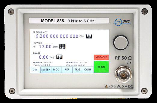
12Connectors
Front (with Touch Screen Display)
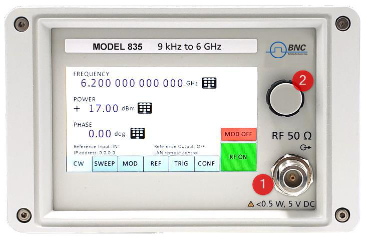
- RF output N female
- Rotary knob
Rear
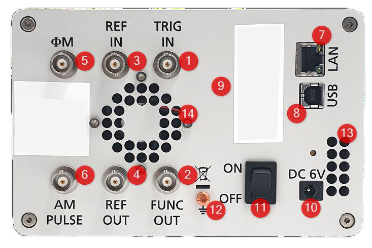
- Trigger input BNC female
- Function output BNC female
- External reference input BNC female
- Internal reference output BNC female
- FM/PM modulation input BNC female
- AM and Pulse modulation BNC female
- LAN connection RJ-45
- USB 2.0 device
- GPIB IEEE-488.2, 1987 with listen and talk (optional)
- DC Power plug (6V, 6 A)
- DC Power switch
- Ground screw
- Vent Holes: Air Intake.
- Vent Holes: Air Exhaust
13Ordering Information
| Host Model | Product / Description |
|---|---|
| 835 | 9 kHz – 4000 MHz Signal Generators |
| 835 | 9 kHz – 6100 MHz Signal Generators |
| 835 | Option B3 Internal rechargeable battery module |
| 835 | Option PE3 Mechanical step attenuator |
| 835 | Option FILT Harmonic Filtering |
| 835 | Option FLASH MicroSD card slot for removable SD memory |
| 835 | Option GPIB GPIB interface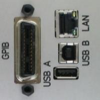 |
| 835 | Option EB6 External power bank adapter cable with voltage converter for 12 to 25 V supply. Required input connector: Inner / outer diameter 2.1 / 5.5 mm |
| 835 | Option AVIO Avionics modulation capability (VOR/ILS) |
| 835 | Option 1URM 1U rack-mount module. Dimensions 1.7 in H x 16.8 in W x 18.1 in L (42 mm H x 426 mm W x 460 mm L)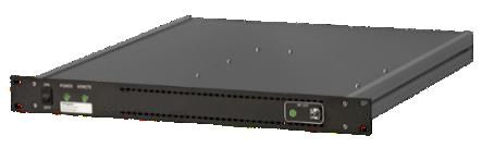 |
| 835 | Option RM 19” 3 U rack-mount kit |
| 835 | Option REAR Move output to the rear panel |
14General Characteristics
| Parameter | Specification |
|---|---|
| Remote Programming Interfaces | Ethernet 100BaseT LAN interface; USB 2.0 host & device; GPIB (IEEE-488.2, 1987) with listen and talk (optional) |
| Control language | SCPI Version 1999.0 |
| Power requirements | 6 VDC; 20 W maximum |
| Mains adapter supplied | 100-240 VAC / 6 V 6.0 A DC out |
| Storage temperature range | -40 to 70 °C |
| Operating temperature range | 0 to 45 °C |
| Operating and storage altitude | up to 15,000 feet |
| Safety / EMC |  complies with applicable Safety and EMC regulations and directives complies with applicable Safety and EMC regulations and directives |
| Weight | 6 lbs (≤2.5 kg) net, 8 lbs (≤ 4 kg) shipping |
| Dimensions (W x L x H), excluding connectors | 6.83 x 9.84 x 4.60 in [172 x 250 x 106 mm] |
| Dimensions (W x L x H), including connectors | 6.83 x 10.66 x 4.60 in [172 x 273 x 106 mm] |
| Recommended calibration cycle | 24 months |
| Compatibility languages | Supporting commonly used commands: Agilent Technologies N5181A MXG, Aeroflex, Rohde & Schwarz SMA and SML models |
15Applications

- R&D Low Noise Signal Source
- Production Testing
- Service and Maintenance
- Signal Simulation
- Aerospace and Defense
- Installation and Maintenance